1 Introduction
With the promotion of radio frequency technology, Mifare1 cards have been widely used in various non-contact communication occasions such as public transportation terminals, handheld terminals, on-board units, and non-contact PC terminals. The contactless smart card reading and writing system is an important part of the RF technology, which can complete many functions such as command analysis and data acquisition. The realization principle of the radio frequency reading and writing system is as follows: a wireless electromagnetic wave of a specific frequency is transmitted from a reader/writer to a Mifare1 card, that is, a radio frequency card. When the RF card is close to the reader, it is excited by the electromagnetic wave emitted by the reader, and the LC resonance circuit in the card resonates and receives electromagnetic wave energy. When the RF card receives sufficient energy, the identification data and other data stored in the card are transmitted to the reader/writer by radio waves and further operations of the data in the card by the reader/writer are accepted.
This paper proposes a design scheme of Mifare1 card reader based on MF RC500. This scheme uses AT89S52 single chip microcomputer to realize the control of MCM (Mifare Core Module). The design of this paper has the advantages of simple hardware implementation and easy secondary development of software. At the same time, due to good electromagnetic compatibility, the system is relatively stable and communication reliability is guaranteed. The overall structure and scheme design of the system are first given below, and then the system is discussed and explained from two aspects: hardware design and software design.
2 system overall structure and design
Fund: National Technology SME Technology Innovation Fund (No.00C26212110519)
This article uses AT89S52 microcontroller, MF RC500 and peripheral circuits to realize the basic components of the reader. The reader and the Mifare1 card are used by the RF field to establish a wireless link and complete data exchange. The overall structure of the system is shown in Figure 1.
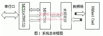
The working mode of the system is mainly to control and communicate with the MF RC500 by the AT89S52, and the MF RC500 drives the peripheral circuit to read and write the Mifare1 card. Specifically, the MCU (microcontroller, ie AT89S52) receives the instructions of the PC through the serial port, completes the operation of the card and the management of the entire reader; the MF RC500 is responsible for the encoding, decoding, signal modulation and solution of the signal. The peripheral circuit establishes the connection between the reader and the RF card. The design of this part directly affects the size of the RF power and the anti-interference ability of the system. The Mifare1 card is the application terminal of the system, receives the command of the reader and returns Instruction execution result.
3 system hardware design
The hardware mainly includes peripheral circuits such as micro-chip MCU, MF RC500, clock circuit, matching circuit and interface. A detailed description of each part and related designs are given below.
(1) MCU part
The system uses a low-power, high-performance CMOS 8-bit microcontroller AT89S52. The chip contains 8k Bytes ISP (In-system programmable) flash read-only program memory that can be erased 1000 times. The device is fabricated using ATMEL's high-density, non-volatile memory technology, compatible with the standard MCS-51 instruction set and 80C51 pin structure, and integrates a general-purpose 8-bit central processor. At the same time, the WATCHDOG with anti-dead lock is on-chip to ensure stable operation of the system.
(2) Base station part
The base unit of the system uses the MF RC500 chip produced by PHILIPS. The MF RC500 is the core component for wireless communication with RF cards, and is the key interface chip for readers to operate Mifare1 cards. It utilizes advanced modulation and demodulation concepts to fully integrate all types of passive contactless communication methods and protocols at 13.56 MHz. The MF RC500 supports all layers of ISO14443A. The internal transmitter section can directly drive the near-operating distance antenna (up to 100mm) without adding active circuitry; the receiver section provides a robust and efficient demodulation and decoding circuit. ISO14443 compatible transponder signal; digital part processing ISO14443A frame and error detection (parity & CRC). In addition, it supports the fast CRYPTO1 encryption algorithm for verifying the Mifare family of products. The convenient parallel interface allows direct connection to any 8-bit microprocessor, providing great flexibility in the design of readers and terminals.
The internal EEPROM of the MF RC500 is divided into four parts, which are used to store product related information, store the register initialization startup file, and store the encryption operation key. The 8 x 64 bit FIFO is used to buffer the input/output data stream between the microcontroller and the chip, and can handle data streams up to 64 bytes in length. The interrupt request of the chip has six kinds of timing setting, sending request, receiving request, one command execution, FIFO full, and FIFO empty. There is a timer in the MF RC500. The clock is derived from the 13.56MHz crystal oscillator signal, and the 13.56MHz signal is generated by the external quartz crystal of the crystal oscillator circuit. The microprocessor can manage the timing tasks with the aid of a timer. The timer can be used for timing output counting, watchdog counting, stop monitoring, timing triggering, etc.
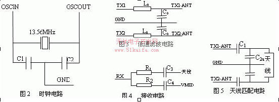
(3) Clock circuit
The MF RC500 integrates an oscillator buffer internally to connect an external 13.56MHz quartz oscillator crystal for low phase jitter, as shown in Figure 2. Since the clock supplied to the MF RC500 is used as the time base for the encoder and decoder of the synchronous system, frequency stability is an important factor in proper implementation. For best performance, the clock jitter should be as small as possible.
(4) Matching circuit
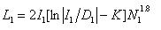
The matching circuit includes an EMC low pass filter, a receiving circuit, an antenna matching circuit, and an antenna.
EMC low-pass filter circuit: The MIFARE system operates at 13.56MHz. The quartz crystal generates the fundamental frequency of the 13.56MHz energy carrier used to drive the MF RC500 and act as the drive antenna. This produces higher harmonics than this frequency, so The output signal must be properly filtered. The low pass filter components include L0 and C0, as shown in Figure 3.
Receiving Circuit: The internal receiving portion of the MF RC500 uses an adjustment of the concept of the card loading response benefiting from the double band of the subcarrier, so the internally generated VMID potential can be used as the input potential of the RX pin. In order to provide a stable reference voltage, a capacitor to ground must be connected to the VMID pin, as shown in Figure 4.
Antenna matching circuit: The component parameters are related to the electrical characteristics and environment of the antenna. The circuit is shown in Figure 5.
Antenna: In antenna design, the most important thing is to calculate the inductance of the antenna coil to determine the antenna bypass capacitor and resistance. The empirical formula is generally used to estimate the inductance of the coil. Assuming the antenna is designed for a common loop or rectangle, there are:
In the formula, The length of one turn of the conductor loop;
The diameter of the wire or the width of the conductor on the PCB;
Antenna shape factor
=1.07, rectangular antenna
=1.47);
The number of laps.
(5) Interface circuit between MF RC500 and MCU
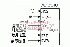
The MF RC500 supports direct interface to different microprocessors, including MCU connections for independent read and write strobes, MCU connections for common read and write strobes, and MCU connections with common read and write strobe and hook functions. After each power-up or hardware reset, the MF RC500 also resets its parallel microprocessor interface mode and automatically detects the type of current microprocessor interface.
The system uses MCU connection mode with common read and write strobe and hook function. Figure 6 shows the interface principle between MF RC500 and MCU. As can be seen from the figure, the system uses the interrupt (INT1) mode of operation, that is, the MCU uses MFRC500 to provide interrupt information to control it. In addition, according to the needs of the system, the MF RC500 can be operated by query.
4 system software design
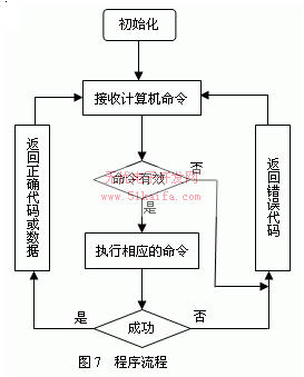
The software design mainly includes initializing the MF RC500, receiving the command of the host computer, controlling the MF RC500, and feeding back the status information of the MF RC500 to the computer. The program flow is shown in Figure 7.
(1) Initialize the parallel interface
First read the Command register until the 6-bit value of the Command is 00H, the internal initialization phase ends, the MF RC500 is ready to receive control; write 80H to the Page register to initialize the microprocessor interface; read the Command register, if the value is 00H, then The processor interface was successfully initialized; the linear address mode was activated by writing 0X00 to the page register after the interface was initialized. This process can be represented by the following code:
Do{PReset=1; Delay(10); PReset=0;} // give reset pulse
While (ReadRC(RegPage) != 0x80);
Do{ WriteRC(RegPage,0x0);}
While(ReadRC(RegCommand) != 0x00);
If (ReadRC(RegCommand) != 0x00)
Status = MI_INTERFACEERR; / / interface initialization error
Else
Status = 0; //Interface successfully initialized
(2) Operation of the Mifare1 card
The commands that the MCU operates on the Mifare1 card are mainly available for operation, loading passwords, verifying passwords, reading cards, writing cards, and checkpoints. No matter which operation, you must first write the command code to the Command register. For example, to execute the verification password, you need to execute the WriteRC (RegCommand, 0x0c) command.
From the operational flow, the operation of the Mifare1 card can be divided into the following items:
Reset request: When a Mifare1 card is within the working range of the reader antenna, the reader issues a REQUEST all (or REQUEST std) command to the card. The ATR of the card will be activated, and the card type (TagType) number in the card Block 0 is transmitted to the reader/writer in a total of 2 bytes, and the first communication communication between the card and the reader is established. If the reset request operation is not performed, the reader's other operations on the card will not proceed.
Anti-collision operation: If there are multiple Mifar1e cards in the working range of the reader antenna, the reader first communicates with each card to obtain the ID number of each card. Since each Mifare1 card has a unique ID number, the reader ensures that only one card is operated at a time based on the ID number of the card.
Card selection operation: After completing the above two steps, the reader must select the card. After performing the operation, return the SIZE byte on the card.
Authentication operation: After the above three steps, when confirming that a card has been selected, the reader must authenticate the password already set on the card. If it matches, further read and write operations are allowed.
Read and write operations: operations such as reading, writing, adding, depreciating, storing, and transmitting cards.
5 Conclusion
The innovative work of this paper: Based on the MF RC500 chip produced by PHILIPS, a design and implementation scheme of a universal RF card reader combined with a single-chip AT89S52 is proposed. The system realizes the reading and writing operation of the Mifare1 card, and has the following advantages: (1) Since the interface mode is relatively large, the operation of the IO port is simple, and the MF RC500 can be conveniently controlled and the corresponding information is obtained; (2) due to the system In the case of reasonable antenna design, the reliability is relatively high, and the effective distance can reach 10cm. (3) The computer can only operate the card by sending commands in a certain way. On this basis, the corresponding can be developed according to different needs. Software products have great practical value.
The practical application shows that the reader/writer architecture has the remarkable advantages of fast response speed, simple use, long card reading distance and stable and reliable communication.
Salon Nails Kit,Golden French Gray False Nails,Short Square Artificial Nails,Super Thin Short False Nails
Zhong Shan Senboma Artware Co.,Ltd , https://www.senbomanails.com